- 您现在的位置:买卖IC网 > Sheet目录369 > X28C512JIZ-12 (Intersil)IC EEPROM 512KBIT 120NS 32PLCC
�� �
�
�X28C512,� X28C513�
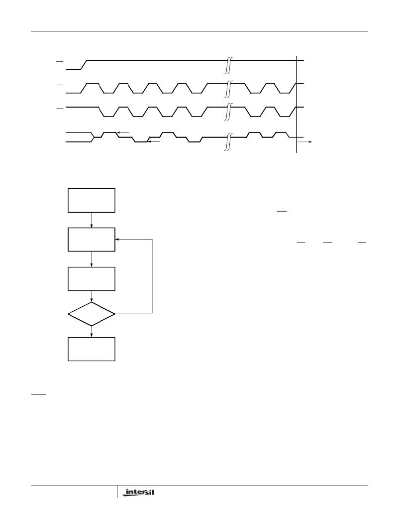
�The� Toggle� Bit� I/O� 6�
�Last�
�WE� Write�
�CE�
�OE�
�I/O� 6�
�*�
�V� OH�
�V� OL�
�HIGH� Z�
�*�
�X28C512,� X28C513�
�Ready�
�*� Beginning� and� ending� state� of� I/O� 6� will� vary.�
�FIGURE� 3A.� TOGGLE� BIT� BUS� SEQUENCE�
�Hardware� Data� Protection�
�Last� Write�
�Load� Accum�
�From� Addr� N�
�Compare�
�Accum� with�
�Addr� N�
�The� X28C512,� X28C513� provide� three� hardware� features�
�that� protect� nonvolatile� data� from� inadvertent� writes.�
�-� Noise� Protection—A� WE� pulse� typically� less� than� 10ns�
�will� not� initiate� a� write� cycle.�
�-� Default� V� CC� Sense—All� write� functions� are� inhibited�
�when� V� CC� is� 3.6V.�
�-� Write� Inhibit—Holding� either� OE� LOW,� WE� HIGH,� or� CE�
�HIGH� will� prevent� an� inadvertent� write� cycle� during�
�power-up� and� power-down,� maintaining� data� integrity.�
�Write� cycle� timing� specifications� must� be� observed�
�concurrently.�
�Software� Data� Protection�
�The� X28C512,� X28C513� offer� a� software� controlled� data�
�Compare�
�Ok?�
�Yes�
�X28C512�
�Ready�
�No�
�protection� feature.� The� X28C512,� X28C513� are� shipped�
�from� Intersil� with� the� software� data� protection� NOT�
�ENABLED;� that� is,� the� device� will� be� in� the� standard�
�operating� mode.� In� this� mode� data� should� be� protected�
�during� power-up/-down� operations� through� the� use� of�
�external� circuits.� The� host� would� then� have� open� read� and�
�write� access� of� the� device� once� V� CC� was� stable.�
�The� X28C512,� X28C513� can� be� automatically� protected�
�FIGURE� 3B.� TOGGLE� BIT� SOFTWARE� FLOW�
�The� Toggle� Bit� can� eliminate� the� chore� of� saving� and�
�fetching� the� last� address� and� data� in� order� to� implement�
�DATA� Polling.� This� can� be� especially� helpful� in� an� array�
�comprised� of� multiple� X28C512,� X28C513� memories� that�
�are� frequently� updated.� Toggle� Bit� Polling� can� also� provide� a�
�method� for� status� checking� in� multiprocessor� applications.�
�The� timing� diagram� in� Figure� 3A� illustrates� the� sequence� of�
�events� on� the� bus.� The� software� flow� diagram� in� Figure� 3B�
�illustrates� a� method� for� polling� the� Toggle� Bit.�
�7�
�during� power-up� and� power-down� without� the� need� for�
�external� circuits� by� employing� the� software� data� protection�
�feature.� The� internal� software� data� protection� circuit� is�
�enabled� after� the� first� write� operation� utilizing� the� software�
�algorithm.� This� circuit� is� nonvolatile� and� will� remain� set� for�
�the� life� of� the� device� unless� the� reset� command� is� issued.�
�Once� the� software� protection� is� enabled,� the� X28C512,�
�X28C513� are� also� protected� from� inadvertent� and� accidental�
�writes� in� the� powered-up� state.� That� is,� the� software�
�algorithm� must� be� issued� prior� to� writing� additional� data� to�
�the� device.� Note:� The� data� in� the� three-byte� enable�
�sequence� is� not� written� to� the� memory� array.�
�FN8106.2�
�June� 7,� 2006�
�发布紧急采购,3分钟左右您将得到回复。
相关PDF资料
X28HC256SIZ-90
IC EEPROM 256KBIT 90NS 28SOIC
X28HC64JIZ-90
IC EEPROM 64KBIT 90NS 32PLCC
XCARD XK-1A
DEV KIT EVENT-DRIVEN PROC XS1-L1
XCARD XTAG-2
ADAPTER USB DEBUGGER JTAG XSYS2
XE8000EV101
EVAL BOARD FOR XE8801AMI027LF
XG4E-6431-S012
CONN PLUG 64POS 1A OPENED COVER
XLNRC
RAPID OUTPUT CONNECTOR
XLT80PT3
SOCKET TRAN ICE 80MQFP/TQFP
相关代理商/技术参数
X28C512JIZ-15
制造商:INTERSIL 制造商全称:Intersil Corporation 功能描述:5V, Byte Alterable EEPROM
X28C512JM-12
制造商:INTERSIL 制造商全称:Intersil Corporation 功能描述:5V, Byte Alterable EEPROM
X28C512JM-15
制造商:INTERSIL 制造商全称:Intersil Corporation 功能描述:5V, Byte Alterable EEPROM
X28C512JM-20
制造商:INTERSIL 制造商全称:Intersil Corporation 功能描述:5V, Byte Alterable EEPROM
X28C512JM-25
制造商:INTERSIL 制造商全称:Intersil Corporation 功能描述:5V, Byte Alterable EEPROM
X28C512JM-90
制造商:XICOR 制造商全称:Xicor Inc. 功能描述:5 Volt, Byte Alterable E2PROM
X28C512JMB-12
制造商:XICOR 制造商全称:Xicor Inc. 功能描述:5 Volt, Byte Alterable E2PROM
X28C512JMB-15
制造商:XICOR 制造商全称:Xicor Inc. 功能描述:5 Volt, Byte Alterable E2PROM